


Grain Boundaries and Stresses: Microchip Component Failure and Electromigration

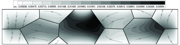
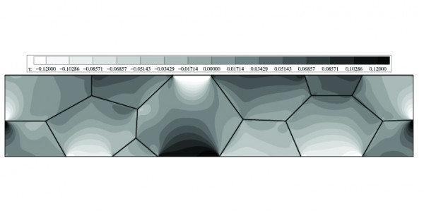
We developed a continuum model of mass transport phenomena in microelectronic circuits due to high current densities (electromigration) and gradients in normal stress along grain boundaries. As microelectronic circuits become smaller and current densities become higher, failure due to electromigration damage is an ever-increasing problem in the design of circuits. Our work, performed in close collaboration with physicists and materials scientists at Motorola, is the first systematic study of the self-consistency and well-posedness of the equations and boundary conditions for stress-grain evolution in microconnect failures.
About Berkeley Lab
Founded in 1931 on the belief that the biggest scientific challenges are best addressed by teams, Lawrence Berkeley National Laboratory and its scientists have been recognized with 16 Nobel Prizes. Today, Berkeley Lab researchers develop sustainable energy and environmental solutions, create useful new materials, advance the frontiers of computing, and probe the mysteries of life, matter, and the universe. Scientists from around the world rely on the Lab’s facilities for their own discovery science. Berkeley Lab is a multiprogram national laboratory, managed by the University of California for the U.S. Department of Energy’s Office of Science.
DOE’s Office of Science is the single largest supporter of basic research in the physical sciences in the United States, and is working to address some of the most pressing challenges of our time. For more information, please visit energy.gov/science.