


Etching and Deposition in Semiconductor Process Manufacturing
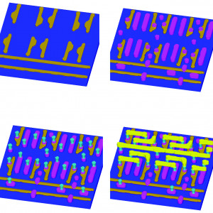
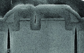
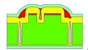
We built a complete suite of mathematical and algorithmic tools to model etching and deposition in semiconductor manufacturing. Level set methods for interface motion are coupled to empirical flux laws, material-depending etch and deposition rates, re-emission profiles and pattern masks. These allow tracking of complex interfaces in plasma-enhanced chemical vapor deposition, ion-milling, and photolithography. Results were validated through careful comparison with experiment, and show the development of voids, needle-structures, three-dimensional faceting in sputter etching and deposition, and angle-dependent reemission profiles. These algorithms are now used worldwide to model the design and manufacture of semiconductors.
About Berkeley Lab
Founded in 1931 on the belief that the biggest scientific challenges are best addressed by teams, Lawrence Berkeley National Laboratory and its scientists have been recognized with 16 Nobel Prizes. Today, Berkeley Lab researchers develop sustainable energy and environmental solutions, create useful new materials, advance the frontiers of computing, and probe the mysteries of life, matter, and the universe. Scientists from around the world rely on the Lab’s facilities for their own discovery science. Berkeley Lab is a multiprogram national laboratory, managed by the University of California for the U.S. Department of Energy’s Office of Science.
DOE’s Office of Science is the single largest supporter of basic research in the physical sciences in the United States, and is working to address some of the most pressing challenges of our time. For more information, please visit energy.gov/science.