


CRD's Shalf Ponders the Future of HPC Architectures in ISC19 Keynote
June 17, 2019
Contact: Kathy Kincade, kkincade@lbl.gov, +1 510 495 2124
What will scientific computing at scale look like in 2030? With the impending demise of Moore’s Law, there are still more questions than answers for users and manufacturers of HPC technologies as they try to figure out what their next best investments should be. As he prepared to head to ISC19 in Frankfurt, Germany to give a keynote address on the topic, John Shalf – who leads the Computer Science Department in Berkeley Lab’s Computational Research Division – shared his thoughts on what the future holds for computing technologies and architectures in the era beyond exascale. ISC takes place June 16-20; Shalf's keynote is on Tuesday, June 18.
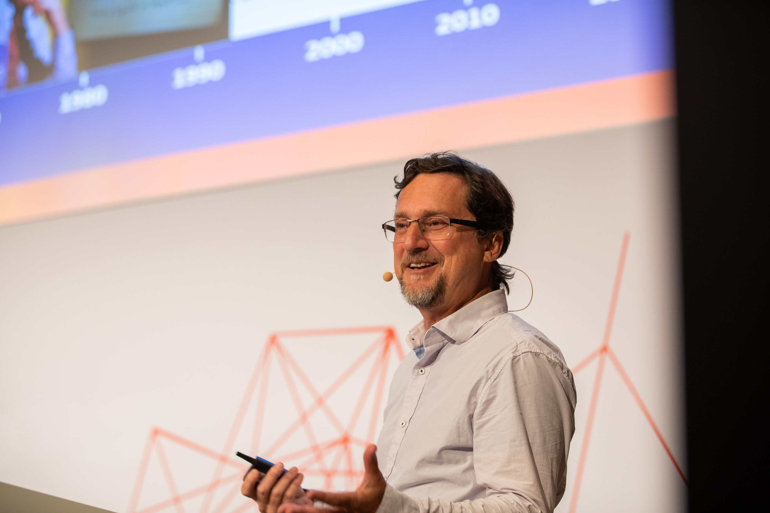
John Shalf explores the post-Moore future of computing in a keynote delivered at ISC19.
What is the focus of your keynote at ISC?
What the landscape of computing, in general, is going to look like after the end of Moore’s Law. We’ve come to depend on Moore’s Law and to really expect that every generation of chips will double the speed, performance, and efficiency of the previous generation. Exascale will be the last iteration of Moore’s Law before the bottom drops out – and the question then is, how do we continue? Is exascale the last of its kind, or are we going to embark on a first-of-its-kind machine for the future of computing?
How long have you been thinking/talking about what’s next for HPC after Moore’s Law?
Where we are now is really the second shoe dropping. I got involved in the Exascale Computing Initiative discussions back in 2008, but actually, my interest in this predates exascale. Back in 2005, David Patterson’s group at UC Berkeley was talking about it in the Parallel Computing Laboratory, and we spent two years there in discussion and debate about the end of Dennard’s scaling. Ultimately we published “The Landscape of Parallel Computing Research: A View from Berkeley,” which was the prediction that parallel computing would become ubiquitous on account of clock frequencies no longer scaling at exponential rates. This was followed closely by the DARPA 2008 Exascale report that set the stage for the Exascale Initiative for HPC. So the end of Dennard’s scaling was the first shoe to drop, but we always knew that the second shoe would drop fairly soon after the first. And the second shoe dropping means we can’t shrink transistors at all anymore, and that is the real end of Moore’s Law. Exascale is addressing the mass parallelism from the first shoe dropping, and I’ve been concerned about the second shoe dropping during the entire 10-year ramp-up to the Exascale Computing Initiative and subsequent Project, as were many others who were involved in writing the View from Berkeley report and the DARPA 2008 report.
How is the slowing of Moore’s Law already affecting HPC technologies and the industry itself?
We are seeing already procurement cycles stretching out so that the replacement of machines is happening at a slower pace than it has historically. Eric Strohmaier at Berkeley Lab has been tracking the replacement rate on the TOP500 very closely, and he has seen a noticeable slowdown in system replacement rates. I’ve also heard from our colleagues in industry that this is a troubling development that will affect their business model in the future. But we are also seeing these effects in the mega datacenter space, such as Google, Facebook, and Amazon. Google has actually taken to designing its own chips, specialized for particular parts of their workflow, such as the Tensor Processing Unit (TPU). We will probably see even more specialization in the future, but how this applies to HPC is less clear at this point – and that’s what I would like to get people thinking about during my keynote.
Is the lithography industry experiencing a parallel paradigm shift?
Yes, the lithography industry is also being affected, and something’s going to need to change in the economics for that industry. What we have seen in the past decade is that we’ve gone from nearly a dozen leading-edge fabs down to two. Global Foundries recently dropped out as a leading-edge fab, and Intel has had a huge amount of trouble getting its 10nm fab line off the ground. So clearly there are huge tectonic shifts happening in the lithography market as we speak, and how that will resolve itself ultimately remains unclear.
Do we have to start imagining an entirely new computing technology development and production process?
I think the way in which we select and procure systems is going to have to be revisited. While using user application codes to run benchmarks to assess the performance and usability of emerging systems is a great way for us to select systems today that use general purpose processors, it doesn’t seem to be a very good approach for selecting systems that might have specialized features for science. In the future, we need to be more closely involved in the design of the machines with our suppliers to deliver machines that are truly effective for scientific workloads. This is as much about sustainable economic models as it is a change in the design process. The most conventional or even the most technologically elegant solution might not survive, but the one that makes a lot of money will. But our current economic model is breaking.
Looking ahead, I see three paths going forward. The first is specialization and better packaging – specialization meaning designing a machine for a targeted class of applications. This has already been demonstrated in the successful case of the Google TPU, for example. So that is the most immediate path forward.
Another potential path forward is new transistor technology that replaces CMOS that is much more energy efficient and scalable. However, we know from past experience that it takes about 10 years to get from a lab demo to a production product. There are promising candidates, but no clear replacements demonstrated in the lab, which means we are already 10 years too late for that approach to be adopted by time Moore’s Law fails. We need to dramatically accelerate the discovery process in that area through a much more comprehensive materials-to-systems co-design process.
The third approach is to explore alternative models of computation such as quantum and neuromorphic and other, related approaches. These are all fantastic, but they are really expanding computing into areas where digital computing performs very poorly. They aren’t necessarily replacement technologies for digital general purpose computing; they are merely expanding into areas where digital isn’t very effective to start with. So I think these are worthy investments, but they aren’t the replacement technology. They will have a place, but how broadly applicable they will be is still being explored.
What about the development of new chip materials – what role might they play in the future of HPC architectures?
New materials are definitely part of the CMOS replacement. It’s not just new materials; fundamental breakthroughs in solid-state physics will be required to create a suitable CMOS replacement. The fundamental principle of operation for existing transistor technology cannot be substantially improved beyond what we see today. So to truly realize a CMOS replacement will require a new physical principle for switching, whether electrical, optical, or magnetic switching. A fundamentally new physical principle will need to be discovered and that, in turn, will require new materials and new material interfaces to realize effective and manufacturable solutions.
Are there any positives when you look at what is happening in this field right now?
Yes, definitely there are positives. We believe the co-design processor is going to require not just software and hardware people to collaborate, it is going to require this collaboration to go all the way down into the materials and materials physics level. And for the national laboratories, this is a great opportunity for us to work closely with our colleagues in the materials science divisions of our respective laboratories. I work at a national laboratory because I’m excited by cross-disciplinary collaboration, and clearly, that is the only way we are going to make forward progress in this area. The recent ASCR Extreme Heterogeneity and DOE Microelectronics BRNs show strong interest by DOE in this deep co-design and collaborative research that is really needed in this space. So to that extent, it is kind of an exciting time.
When you think about the future of HPC and supercomputing architectures and technologies, what do you imagine they will look like 10 years from now?
I think we’re going to have smaller machines that are more effective for the workflows they target. For three decades we have become used to ever-growing, larger and larger machines, but that doesn’t seem to be the winning approach for creating effective science in the post-exascale and post-Moore era.
About Berkeley Lab
Founded in 1931 on the belief that the biggest scientific challenges are best addressed by teams, Lawrence Berkeley National Laboratory and its scientists have been recognized with 16 Nobel Prizes. Today, Berkeley Lab researchers develop sustainable energy and environmental solutions, create useful new materials, advance the frontiers of computing, and probe the mysteries of life, matter, and the universe. Scientists from around the world rely on the Lab’s facilities for their own discovery science. Berkeley Lab is a multiprogram national laboratory, managed by the University of California for the U.S. Department of Energy’s Office of Science.
DOE’s Office of Science is the single largest supporter of basic research in the physical sciences in the United States, and is working to address some of the most pressing challenges of our time. For more information, please visit energy.gov/science.